


The rise of inference-optimized chips marks a pivotal shift in AI infrastructure, moving beyond training-centric hardware to specialized silicon designed for cost-effective, low-latency model execution. Driven by explosive growth in generative AI and edge computing, this market is projected to hit $50 billion by 2026. These chips, from giants like NVIDIA and startups alike, prioritize energy efficiency, memory bandwidth, and integer performance to run AI models at scale in data centers, smart factories, and autonomous devices.
Wholesale Server Hardware ; IT Components Supplier ; Wecent
What is driving the explosive market growth for inference chips?
The explosive growth is fueled by the ubiquitous deployment of generative AI and the practical demands of running models post-training. Unlike the intensive, batch-oriented nature of training, inference happens constantly—every chatbot query, image generation, or sensor analysis requires it. This creates an insatiable demand for hardware that’s not just powerful, but also power-sipping and cost-optimized for relentless, real-time processing.
Beyond the hype, the core driver is simple economics. Training a massive model like GPT-4 is a monumental, one-time cost, but serving its predictions to millions of users is a continuous, operational expense. Deploying general-purpose training GPUs for this task is like using a Formula 1 car for daily commuting—overpowered and prohibitively expensive. That’s where inference-optimized chips come in. They are the efficient, scalable workhorses built for this marathon. For instance, a financial services client working with WECENT replaced underutilized A100s in their fraud detection pipeline with purpose-built inference accelerators, slashing their per-transaction compute cost by over 60% while maintaining sub-5ms latency. The shift from building AI to using it everywhere is what’s truly powering this $50B forecast. But what does this mean for enterprise infrastructure? It necessitates a fundamental rethinking of hardware strategy, prioritizing total cost of ownership (TCO) over peak theoretical performance.
How do inference chips differ technically from training chips?
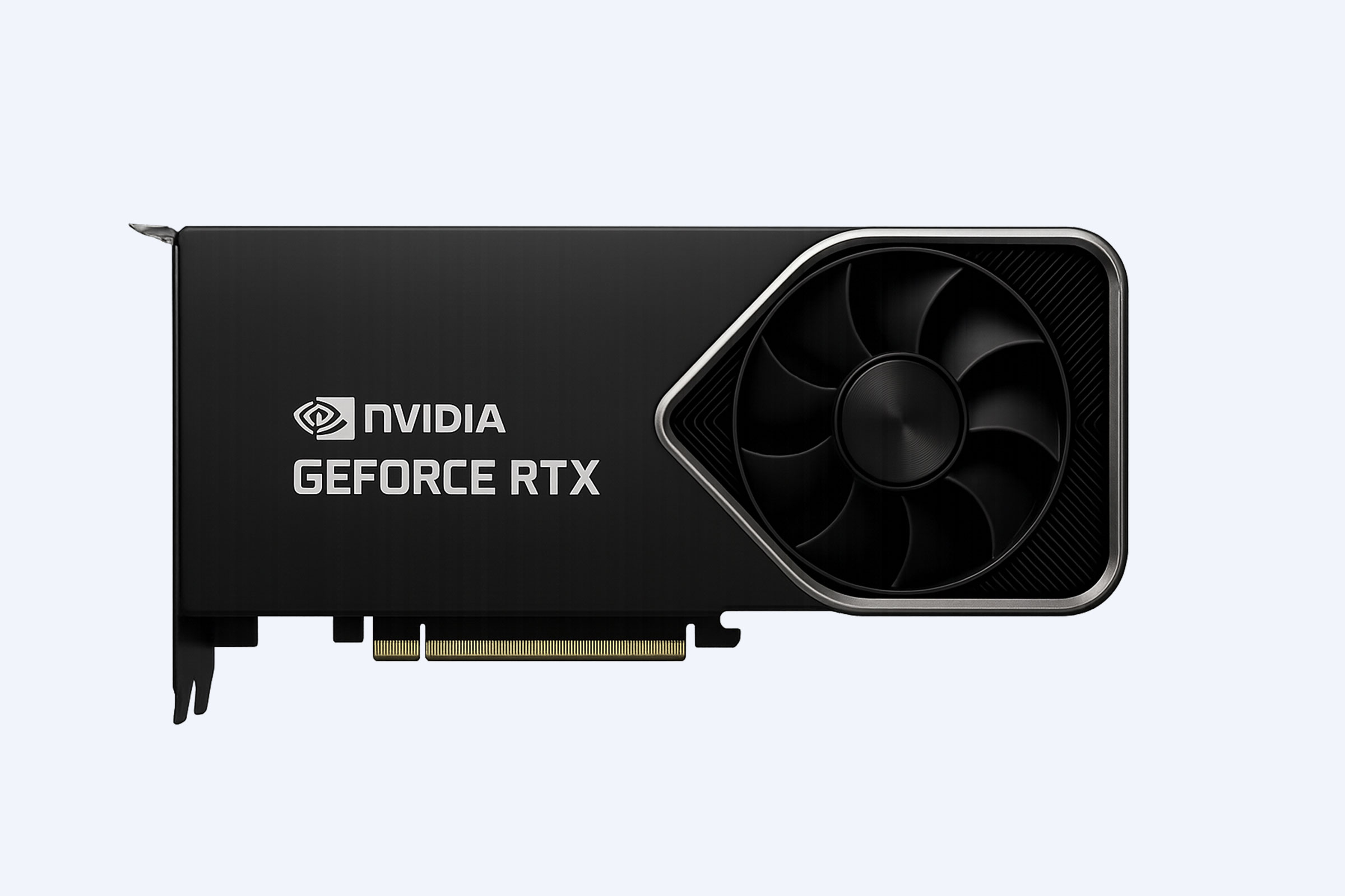
Inference and training chips are architecturally distinct, optimized for different phases of the AI lifecycle. While training chips need massive FP32/FP64 precision and robust error-checking, inference chips prioritize INT8/INT4 operations, memory bandwidth, and ultra-low latency. The goal is to execute a pre-defined model as fast and efficiently as possible, often with lower numerical precision that’s “good enough” for the task.
Think of training a chip as educating a scholar: it requires extensive libraries (high-bandwidth memory), the ability to draft and revise complex theories (high-precision floating-point math), and tolerance for iterative mistakes (robust error correction). Inference, however, is like that scholar answering quiz questions: speed, recall, and efficiency are paramount. Technically, this translates to several key differences. Inference chips often feature larger on-chip SRAM or specialized memory hierarchies to minimize data movement, the primary energy consumer. They integrate more fixed-function units for common operators (like transformers) rather than general-purpose CUDA cores. Practically speaking, a training chip like the NVIDIA H100 is a beast with Tensor Cores for FP8/FP16, while an inference-optimized chip might excel at INT8 throughput. In a real-world WECENT deployment for a video analytics platform, switching from a general-purpose GPU to an inference-optimized ASIC allowed the client to process 4x more video streams per rack, purely due to lower power draw and more efficient integer compute. So, while they may look similar, their internal design philosophies cater to opposite ends of the AI workflow.
| Feature | Training Chip (e.g., NVIDIA H100) | Inference Chip (e.g., NVIDIA L4) |
|---|---|---|
| Primary Precision | FP16, BF16, TF32, FP8 | INT8, INT4, FP16 (sparse) |
| Power Profile | High (500W-700W) | Low to Moderate (72W-300W) |
| Optimization Goal | Throughput & Model Accuracy | Latency & Power Efficiency |
Why is Edge AI a critical catalyst for inference chip design?
Edge AI demands processing data locally on devices, which imposes severe constraints on power, heat, and space. This forces inference chip design toward radical efficiency, spurring innovation in low-power architectures, thermal design power (TDP) management, and model compression techniques. The edge isn’t just a location; it’s a set of extreme engineering requirements.
In the data center, you can throw more power and cooling at a problem. At the edge—in a camera on a factory floor, a vehicle, or a smartphone—you have a strict wattage budget and no room for a liquid cooling loop. This environment is the ultimate proving ground for inference efficiency. Consequently, edge inference chips often leverage specialized neural processing units (NPUs) that outperform general-purpose CPUs/GPUs within a tight power envelope. Beyond raw silicon, the entire software stack must be lean. For example, WECENT’s work with healthcare device integrators involves optimizing models using TensorRT or OpenVINO to run efficiently on low-power Jetson Orin modules for real-time diagnostic imaging. The result? Life-critical inferences happen in milliseconds without relying on a potentially unreliable network connection. So, while data center inference chips focus on throughput, edge chips are obsessed with latency and efficiency. This divergence is creating two vibrant, specialized sub-markets within the broader inference landscape.
What are the key architectural features of a modern inference chip?
Modern inference chips are defined by specialized tensor cores or NPUs, advanced memory subsystems with high bandwidth, and support for sparse computation and variable precision. They often include hardware for transformer engine acceleration and on-chip networking for scalable deployments. The architecture is a holistic answer to the inference bottleneck.
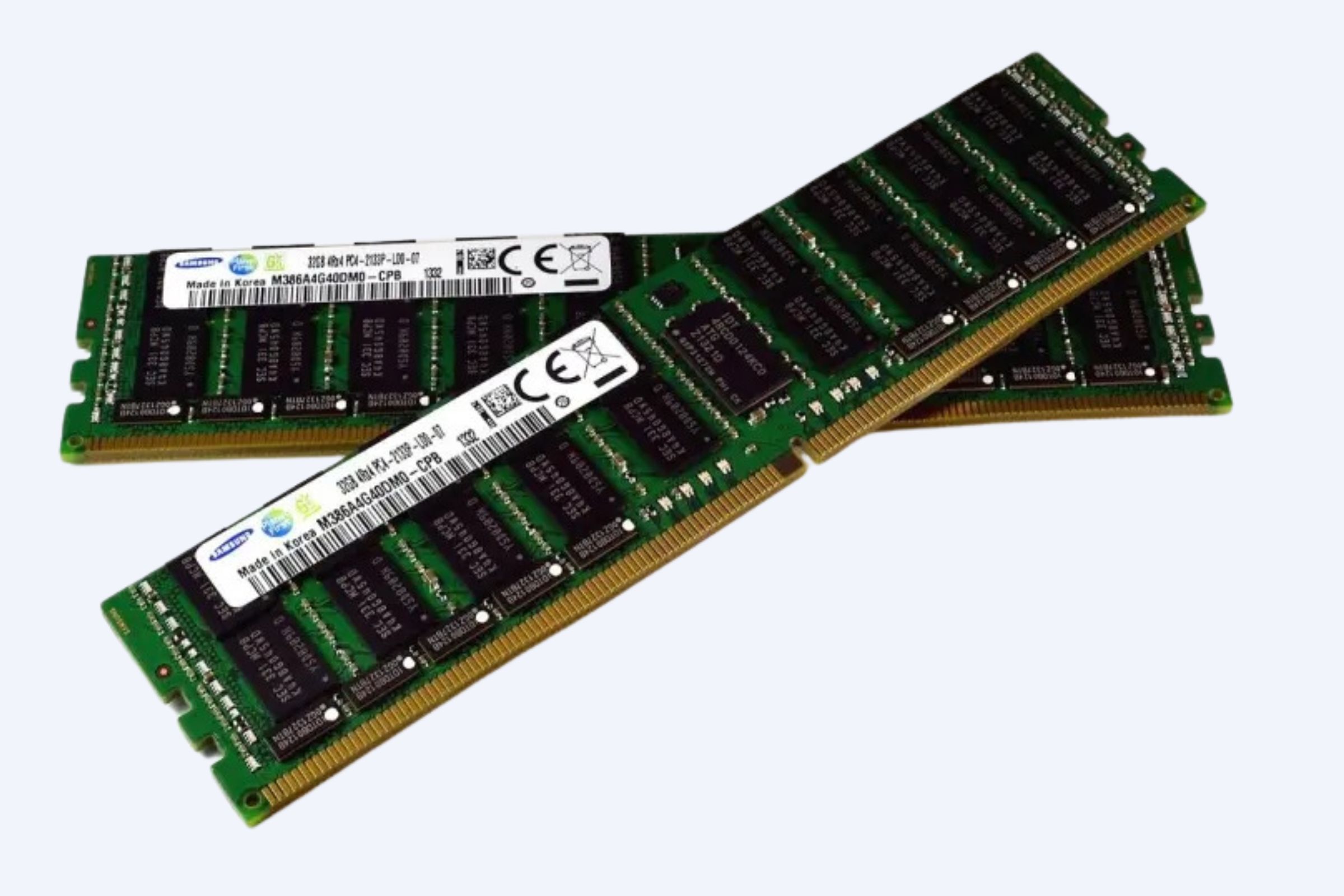
Let’s break down why these features matter. Specialized tensor cores or NPUs execute matrix multiplications—the heart of neural networks—with far greater efficiency than a general-purpose ALU. A sophisticated memory hierarchy, perhaps using HBM3e or large caches, ensures these cores are fed with data continuously, avoiding stalls. Support for sparsity allows the chip to skip computations on zero-value weights, which can be abundant in pruned models, effectively doubling throughput. But how does this translate to real performance? Take a chip with transformer engine acceleration: it can dynamically switch between FP8 and INT8 precision during different layers of a model, maximizing both accuracy and speed. In a recent proof-of-concept with a retail analytics client, WECENT leveraged NVIDIA’s A100 (with its 3rd Gen Tensor Cores and sparsity support) for a hybrid training/inference node. However, for a pure inference rollout, we recommended the H20, which is architected with a higher ratio of INT8 compute, making it more cost-effective for serving the final model. The architecture is always a trade-off, and the best inference chip is the one whose trade-offs align perfectly with your specific model and deployment constraints.
| Architectural Feature | Benefit for Inference | Example in Practice |
|---|---|---|
| Large On-Chip SRAM/Cache | Reduces energy-hungry off-chip memory access, lowering latency and power. | Enables real-time object detection on battery-powered drones. |
| Hardware Sparse Acceleration | Increases effective compute throughput by skipping zero-weight calculations. | Can double the tokens/second in a pruned large language model (LLM). |
| Structured Sparsity | Allows for more predictable performance gains and easier model optimization. | Used in NVIDIA’s Ampere architecture for reliable 2x inference speedups. |
How does the Deloitte report frame the economic impact of this shift?
The Deloitte report frames the shift as a strategic inflection point, highlighting how inference optimization drives democratization of AI and improves total cost of ownership (TCO). It emphasizes that cost-effective inference is the key to scaling AI from pilot projects to pervasive, production-grade applications across all industries. The economic argument is as important as the technical one.
Deloitte’s analysis goes beyond silicon specs to focus on business outcomes. The core thesis is that expensive, centralized training will continue, but the real value extraction happens through ubiquitous, cheap inference. This has a cascading effect: lower inference costs enable new use cases (e.g., AI on every security camera), which generates more data, which can be used to refine models, creating a virtuous cycle. For enterprise leaders, the report is a call to action to scrutinize their AI infrastructure spend. Are you paying for capability you don’t need? In our experience at WECENT, many clients initially overallocate training-grade GPUs to inference tasks. By conducting a workload analysis, we often find that a fleet of lower-cost, inference-optimized L4 or A2 GPUs, or even specialized ASICs, can handle the load at a fraction of the capital and operational expense. This isn’t just about saving money; it’s about making ambitious AI roadmaps financially sustainable. After all, what good is a brilliant AI model if it’s too expensive to run?
What should enterprises consider when building an inference-optimized infrastructure?
Enterprises must consider workload profiling, software ecosystem support, scalability, and total cost of ownership (TCO). It’s not just about buying the fastest chip; it’s about creating a balanced, flexible system where compute, memory, networking, and software work in harmony to serve models reliably and cost-effectively.
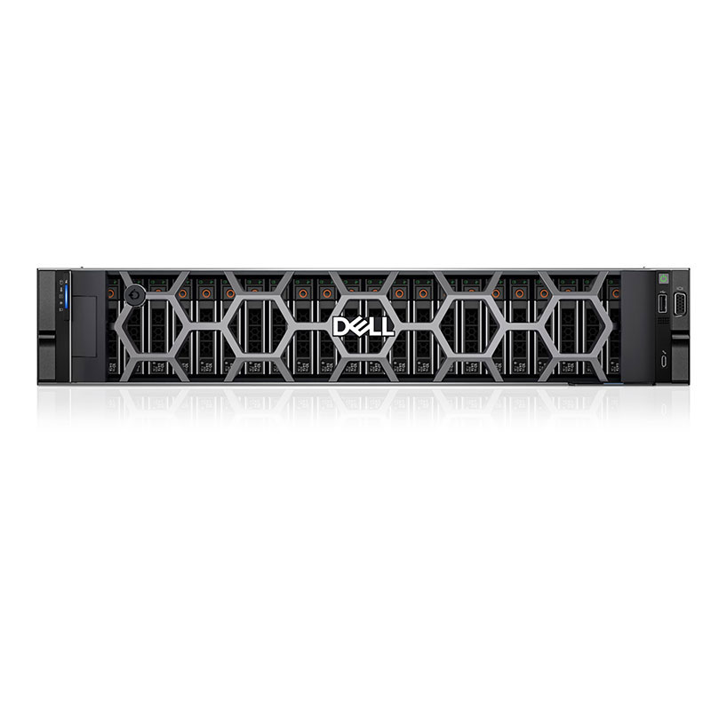
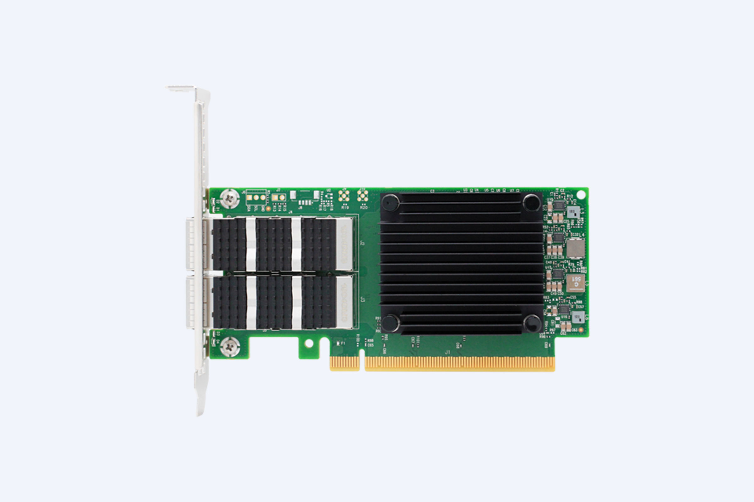
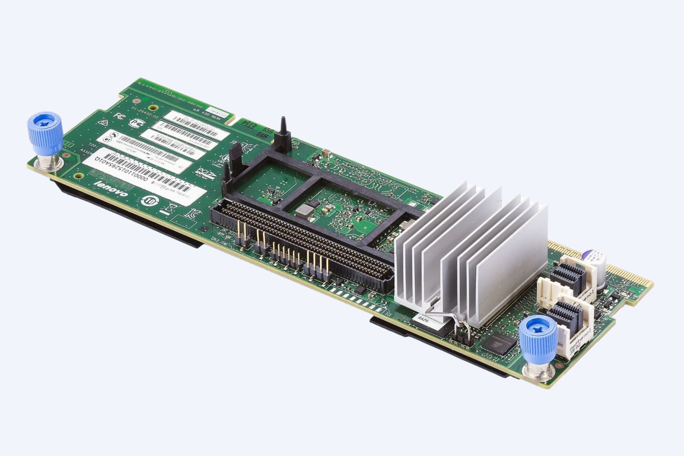
The first step is rigorous workload profiling. What models are you running? What are their precision requirements (FP16, INT8)? What are your latency SLAs and throughput targets? This profile dictates hardware selection. Beyond the chip, you must evaluate the full stack. Does the vendor’s software (drivers, compilers, frameworks like TensorRT) support your models and allow for easy optimization? Furthermore, consider scalability: can you start small and scale out horizontally with efficient networking? A WECENT deployment for an online retailer involved designing a cluster using Dell PowerEdge R760xa servers equipped with multiple low-TDP inference GPUs, interconnected with NVIDIA BlueField DPUs for efficient model serving and network offload. This architecture allowed them to elastically scale inference capacity during peak shopping hours. Ultimately, the goal is to avoid vendor lock-in and create a platform that can adapt to the next generation of models and chips. It’s a complex puzzle, but getting it right is the difference between an AI showcase and an AI-powered competitive advantage.

WECENT Expert Insight
FAQs
Yes, for prototyping or light loads, but they lack enterprise features like ECC memory and optimized inference software stacks. For production-scale, 24/7 reliability, WECENT recommends datacenter-grade GPUs like the L4 or professional RTX A-series with validated drivers and support.
Is it better to have a few powerful inference chips or many smaller ones?
It depends on your scalability model. Many smaller, efficient chips (like L4s) offer better granular scaling and fault tolerance for distributed microservices. A few powerful chips (like H100s) may be better for batched, high-throughput jobs. WECENT can help model both scenarios.
How do I future-proof my inference infrastructure investment?
Focus on flexible, standards-based platforms (like PCIe Gen5 servers) that allow you to swap accelerator cards. Prioritize software agility and choose a supplier like WECENT with direct access to OEM roadmaps, ensuring you can seamlessly integrate next-generation chips as they emerge.