


TSMC’s reported2nm process delays present a significant hurdle for next-generation AI chip production, potentially slowing the pace of AI advancement. This isn’t the end of Moore’s Law for AI, but it signals a critical inflection point where architectural innovation, software optimization, and system-level design must become the primary drivers of performance gains beyond pure transistor scaling.
What is the current status of TSMC’s2nm process technology?
TSMC’s2nm node, known as N2, is in advanced development but facing technical and yield challenges that could push volume production into2026. This delay impacts the roadmap for leading-edge AI accelerators and high-performance computing chips that rely on the density and power efficiency promised by this next-generation semiconductor manufacturing process.
The transition to2nm represents a monumental leap, moving from FinFET transistors to a new Gate-All-Around (GAA) nanosheet transistor architecture. This shift is necessary to continue scaling but introduces immense complexity in fabrication, material science, and defect control. While TSMC has demonstrated test chips, achieving the high yields required for cost-effective mass production of large, complex dies like those used in AI processors is a separate battle. For instance, moving to GAA is like rebuilding the foundation of a skyscraper while it’s still occupied; the potential is vast, but the execution risk is high. The industry is watching closely because a six-month delay can cascade through the entire ecosystem, from chip design to system deployment. How will chip designers adapt their architectures if the promised power and performance benefits are delayed? And what does this mean for the competitive landscape if one foundry stumbles? Consequently, companies are developing contingency plans, exploring multi-die chiplet designs and advanced packaging to mitigate the risk. The timeline remains fluid, and the true impact will be measured by when consistent, high-volume output is achieved.
How do semiconductor process node delays directly impact AI development timelines?
Process node delays create a domino effect, pushing back the tape-out and production schedules for new AI accelerator chips from companies like NVIDIA, AMD, and custom silicon developers. This postpones the availability of more powerful and efficient hardware, which in turn slows the training of larger, more complex AI models and delays the deployment of real-time AI applications that depend on that increased computational throughput.
AI model complexity is growing at a rate that often outpaces hardware gains, a dynamic described by OpenAI’s analysis of computing needs for advanced AI. A delay in the underlying silicon platform means that researchers and engineers hit computational ceilings sooner. Training a frontier large language model today requires thousands of GPUs running for months; the next generation of models will demand even more. Without the efficiency and performance uplift from a new process node, the cost and energy consumption of these projects become prohibitive. Consider the analogy of trying to fuel a new generation of supersonic jets with the same grade of gasoline used by propeller planes; the engine design is ready, but the fuel isn’t powerful enough. This bottleneck forces difficult choices: do you scale out with more, less efficient hardware, or do you delay ambitious research projects? Furthermore, product cycles for consumer devices with AI features, from smartphones to laptops, are often locked to chip release schedules. A foundry delay can therefore ripple from the data center to the edge, affecting a wide array of industries. The immediate impact is a throttling of the raw computational power available to push the boundaries of what’s possible in artificial intelligence.
Which alternative strategies are companies pursuing to advance AI performance beyond transistor scaling?
With physical scaling becoming harder, the industry is aggressively pursuing a multi-faceted approach centered on architectural innovation, advanced packaging, and software-hardware co-design. Key strategies include developing specialized chiplet-based designs, leveraging technologies like CoWoS packaging, creating domain-specific architectures, and implementing sophisticated model compression and software optimization techniques to extract more performance from existing silicon.
| Strategy | Technical Approach | Primary Benefit for AI | Real-World Implementation |
|---|---|---|---|
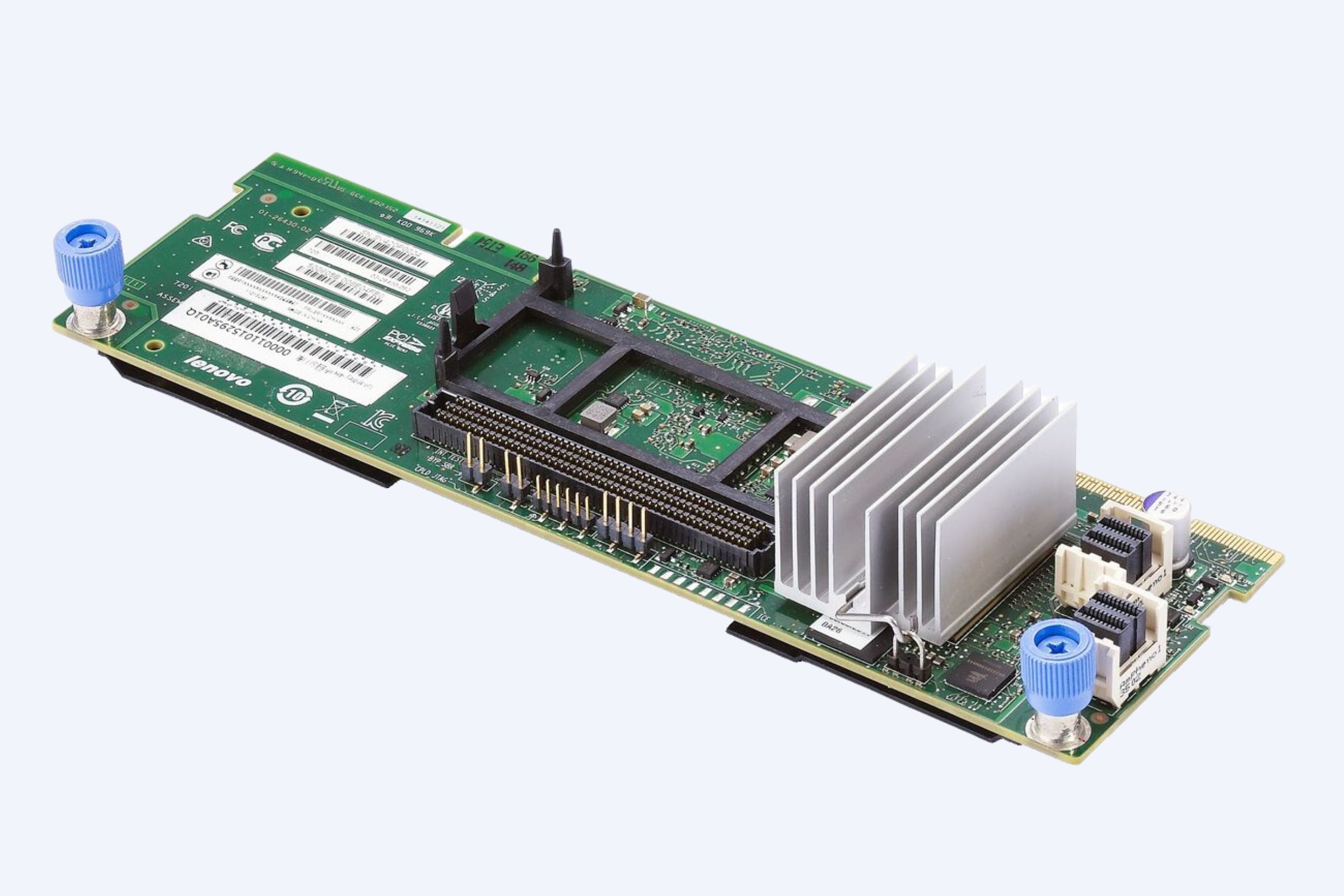
| Chiplet & Advanced Packaging | Disaggregating a large monolithic die into smaller “chiplets” connected via high-density interconnects (e.g., UCIe) and packaged using2.5D/3D tech like CoWoS. | Improves yield, allows mixing process nodes, and enables larger effective die sizes beyond the reticle limit. | AMD’s Instinct MI300 series, Intel’s Ponte Vecchio, and NVIDIA’s own Blackwell B200 GPU utilize complex multi-chiplet designs. |
| Domain-Specific Architecture (DSA) | Designing hardware with fixed-function units optimized for specific AI workloads (e.g., matrix multiplication, tensor cores) rather than general-purpose computing. | Delivers orders of magnitude better performance-per-watt for targeted algorithms compared to general-purpose CPUs or GPUs. | Google’s TPU, AWS Inferentia/Trainium, and the dedicated neural processing units (NPUs) now common in smartphones and laptops. |
| Software & Algorithmic Optimization | Techniques like model pruning, quantization, distillation, and sparsity exploitation to reduce computational load without significant accuracy loss. | Enables larger models to run on current-generation hardware, reducing inference latency and deployment cost. | OpenAI’s GPT-4 inference optimization, PyTorch’s built-in quantization libraries, and NVIDIA’s TensorRT software suite. |
| Novel Materials & Transistor Structures | Research into materials like graphene or2D semiconductors (e.g., MoS2) and new transistor concepts like CFETs for post-silicon eras. | Long-term path to resume density and performance scaling once silicon-based CMOS approaches fundamental limits. | IBM and research consortia demonstrating prototype devices in labs, though years from commercialization. |
Why is the concept of “Moore’s Law” becoming less relevant for measuring AI progress?
Moore’s Law, which observed the doubling of transistors on a chip every two years, is a metric of manufacturing density, not computational capability for specific tasks. AI progress is increasingly gated by factors beyond transistor count: memory bandwidth, interconnect speeds, thermal design power, and the efficiency of algorithms. Therefore, a holistic system-level view, often called “Moore’s Law for Systems,” is now a more accurate benchmark for AI advancement.
The original formulation of Moore’s Law said nothing about performance, cost, or power efficiency—it was purely an observation about component density. In the AI era, simply having more transistors doesn’t guarantee faster training if data cannot be fed to them quickly enough, a problem known as the memory wall. The real metric for AI is the time-to-solution for a given model or the throughput of inferences per joule of energy. This shift in focus is profound. It’s akin to measuring a car’s performance not by engine size alone, but by its lap time on a track, which depends on tires, aerodynamics, and driver skill. Are we reaching the limits of what silicon can do, or are we just reaching the limits of a simplistic, transistor-centric worldview? The industry’s answer is clearly the latter. This is why companies are investing billions in high-bandwidth memory like HBM3e, ultra-fast inter-chip links like NVLink, and liquid cooling solutions. The performance of a modern AI server from a supplier like WECENT is a symphony of coordinated components, not just a solo act by the processor. The end of classic Moore’s Law doesn’t mean the end of progress; it means the rules of the game have changed.
How can businesses plan their AI infrastructure investments in light of these semiconductor uncertainties?
Businesses should adopt a flexible, hybrid strategy that avoids over-reliance on any single, future hardware generation. This involves architecting software for portability across hardware platforms, investing in scalable, composable infrastructure that can integrate new accelerators as they become available, and prioritizing total cost of ownership and energy efficiency over chasing peak theoretical performance from unproven next-generation silicon.
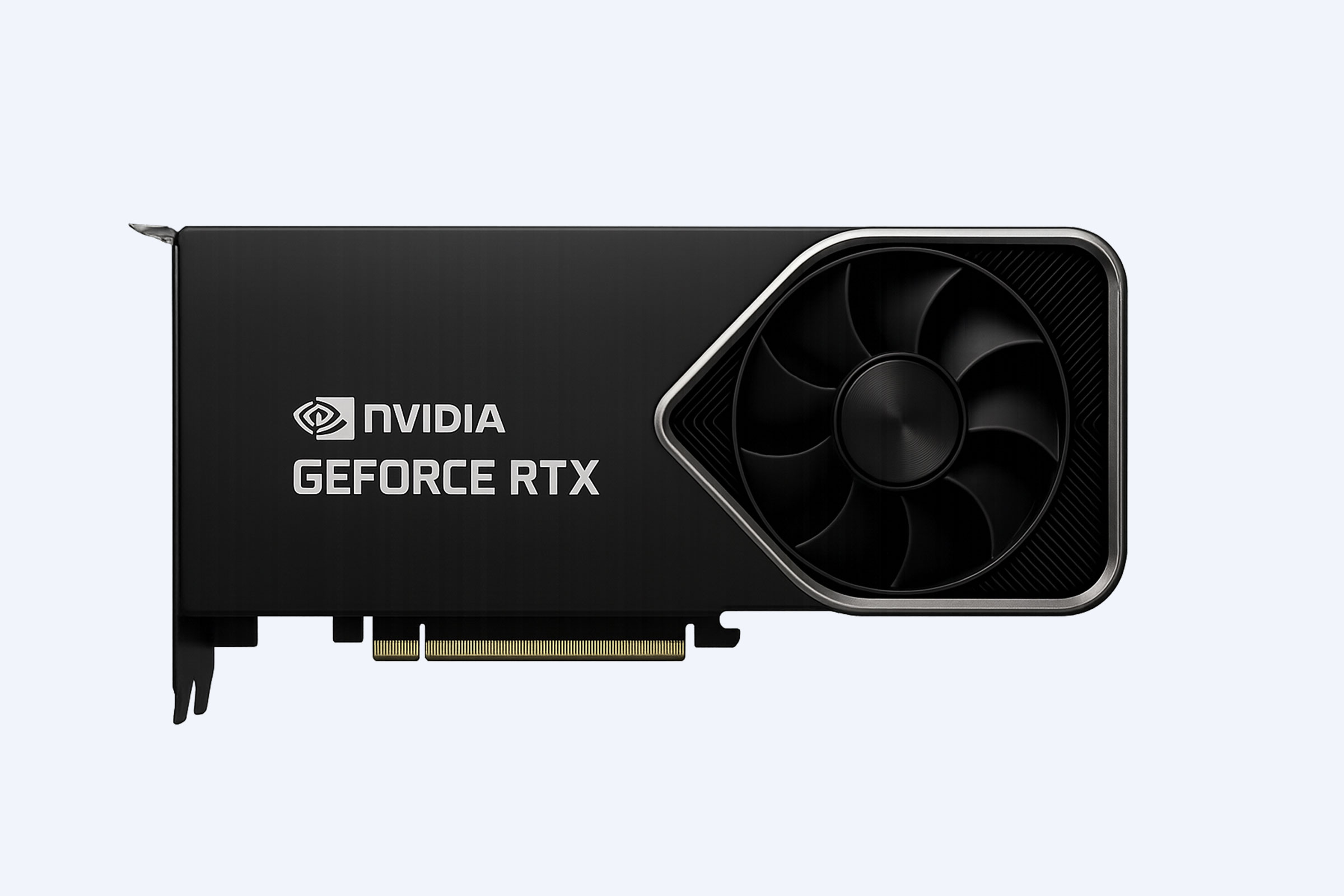
The key is to build resilience into your AI roadmap. Instead of betting your entire strategy on the timely arrival of a specific2nm-based chip, design your systems and workflows to be agnostic where possible. Utilize containerization and orchestration platforms like Kubernetes to abstract workloads from the underlying hardware. This allows you to deploy on today’s proven platforms, such as NVIDIA’s Hopper-based H100 systems, with the ability to seamlessly incorporate Blackwell or other architectures later. Partnering with an experienced IT solutions provider like WECENT can be invaluable here, as they can provide insights into stable supply chains for current-generation equipment and guidance on scalable infrastructure designs. For example, opting for a modular server platform that allows for GPU upgrades without a full system replacement can protect your capital investment. What is the operational cost of waiting for delayed hardware versus deploying a slightly less efficient solution today that can start generating value immediately? The answer often favors immediate, pragmatic deployment. Focus on solving business problems with available technology, using software optimization to stretch your hardware further, and building a financial model that accounts for the volatility in the semiconductor sector.
What does the competitive landscape for AI chips look like beyond TSMC’s foundry dominance?
The landscape is diversifying as companies seek to mitigate supply chain risk and leverage alternative technologies. While TSMC remains the leader, competitors like Samsung Foundry and Intel Foundry Services are aggressively pursuing their own2nm-class processes. Furthermore, the rise of custom silicon designed by hyperscalers (Google, Amazon, Meta) and the growth of open architectures (RISC-V) are creating a more fragmented but innovative ecosystem less dependent on a single company’s roadmap.
| Competitor/Approach | Key Technology & Status | Potential Impact on AI Chip Supply | Notable Partners/Designs |
|---|---|---|---|
| Samsung Foundry | Developing SF2 (2nm) with GAA, aiming for production in2025. Has been a secondary source for some NVIDIA and other fabless chips. | Provides a crucial alternative source for advanced manufacturing, increasing capacity and supply chain resilience for the industry. | Historically manufactured NVIDIA’s8nm GPUs; competing for future NVIDIA, AMD, and Qualcomm business. |
| Intel Foundry Services (IFS) | Aggressively executing its “5 nodes in4 years” plan. Its20A and18A (roughly2nm-class) nodes with RibbonFET GAA and PowerVia backside power delivery are key offerings. | Seeks to become a major foundry player, potentially attracting companies wanting geographic and supplier diversity, especially in the US. | Will manufacture high-performance chips for Microsoft; attracting interest from other major fabless designers. |
| Hyperscaler Custom Silicon | Companies like Google, Amazon, and Meta design their own AI accelerators (TPU, Trainium, MTIA) and often work with multiple foundries for production. | Reduces demand pressure on commercial AI GPU supply and drives architectural innovation tailored to specific data center workloads. | Google’s TPU v5, Amazon’s Trainium2, and Meta’s MTIA are all built for internal use, shaping cloud AI service offerings. |
| Open Architecture (RISC-V) | Open-source instruction set architecture enabling custom, domain-specific core designs without architectural licensing fees. | Lowers barriers to entry for AI chip startups, fostering innovation in specialized accelerators for edge AI and niche applications. | Startups like Tenstorrent and established players exploring RISC-V for AI workloads alongside Arm and x86. |
Expert Views
“The narrative around Moore’s Law ‘ending’ is a distraction. What we’re witnessing is its evolution from a purely transistor-centric phenomenon to a system-level challenge. The future of AI computing will be defined by heterogeneity—the co-design of specialized silicon, advanced packaging, memory hierarchies, and purpose-built software stacks. Companies that master this full-stack integration will lead the next decade, regardless of the nanometer label on the process node. Delays at the leading edge simply accelerate the investment and focus on these other, equally critical vectors of innovation. For enterprises, this means performance gains will come from smarter system design, not just a wait for the next chip shrink.”
Why Choose WECENT
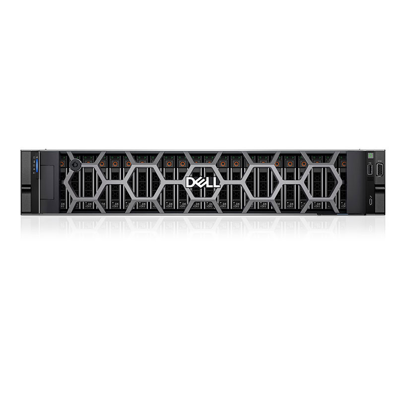
Navigating the complexities of modern AI infrastructure requires a partner with deep technical expertise and a broad view of the hardware landscape. WECENT brings over eight years of experience as a professional IT equipment supplier, offering access to original, high-quality servers and components from leading global brands. Our value lies in providing unbiased guidance tailored to your specific AI workload requirements, whether you need to deploy a scalable cluster of current-generation NVIDIA GPUs or plan a future-proof system architecture that can adapt to new accelerators. We understand that the foundation of any successful AI project is reliable, performant, and efficiently supported hardware. Our focus is on delivering the stable building blocks—from PowerEdge servers to certified GPUs and storage—that allow your team to focus on innovation, not infrastructure uncertainty. By partnering with WECENT, you gain a resource that helps you make informed decisions based on real-world performance data and supply chain awareness, ensuring your investments are sound even amidst industry shifts.
How to Start
Begin by conducting a thorough assessment of your current and projected AI workloads. Define clear metrics for success, such as model training time, inference latency targets, and budget constraints. Next, engage with technical experts to translate these requirements into a preliminary architectural design, considering factors like GPU memory bandwidth, server node interconnectivity, and storage I/O. This is where a consultation with a solutions provider like WECENT can provide practical insights into available hardware options and their trade-offs. The third step is to prototype a small-scale proof-of-concept using a representative workload on the proposed infrastructure to validate performance and identify bottlenecks. Finally, based on the results, finalize your design and develop a phased deployment and scaling plan, ensuring your infrastructure strategy includes a roadmap for software optimization and potential hardware refreshes as new technologies mature and become commercially stable.
FAQs
No, development will not stall. While leading-edge research pushing the absolute limits of model size may be impacted, the vast majority of commercial and applied AI work will continue. The industry will rely more heavily on the alternative strategies discussed, such as software optimization, efficient model architectures, and scaling out with current-generation hardware, to maintain progress.
For most businesses, postponement is not advisable. The time-to-value gained by deploying proven, available technology today typically outweighs the benefits of waiting for future hardware, especially given uncertain timelines. Building expertise and solving problems now with current platforms positions you better to leverage next-generation hardware when it eventually arrives.
WECENT assists clients by designing for modularity and upgradeability from the start. We recommend server platforms with flexible I/O and expansion capabilities, advocate for composable infrastructure principles where possible, and provide lifecycle management services. This approach allows clients to incrementally upgrade components like GPUs or storage, protecting their core infrastructure investment over a longer period.
Chiplets are a powerful and promising strategy, but not a guaranteed panacea. They introduce their own complexities in design partitioning, high-speed interconnect, and thermal management. However, they are currently the most viable path forward for continuing performance scaling, as evidenced by their adoption by all major players, and they do mitigate some of the risks associated with monolithic die scaling.
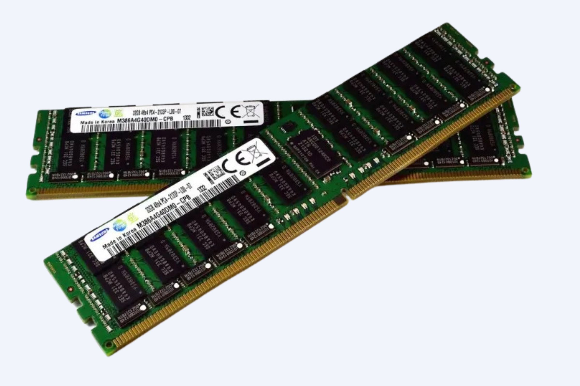
There is no single factor; it is the balance and integration of multiple elements. However, memory bandwidth and capacity are increasingly critical bottlenecks. The ability to quickly feed data to massively parallel processors often limits overall system performance more than the raw compute power of the processors themselves, making technologies like HBM essential.
In conclusion, the reported delays at TSMC are a significant event, but they represent a shift in the drivers of AI progress rather than its cessation. The key takeaway is that future gains will be achieved through a more holistic approach encompassing novel chip architectures, sophisticated software, and intelligent system design. For businesses, the actionable advice is to prioritize flexibility and total cost of ownership, build infrastructure that can evolve, and partner with knowledgeable experts who can guide you through a period of transition. By focusing on solving real problems with available, robust technology and maintaining an adaptable strategy, organizations can continue to leverage AI for competitive advantage regardless of the nanometer timeline.