


Meta’s MTIA v2 is a custom AI accelerator chip designed for production-scale inference workloads, aiming to reduce reliance on third-party GPUs. It leverages a multi-core architecture with specialized tensor processing units and high-bandwidth memory to optimize efficiency for Meta’s specific AI models, such as ranking and recommendation engines, within its massive data centers.
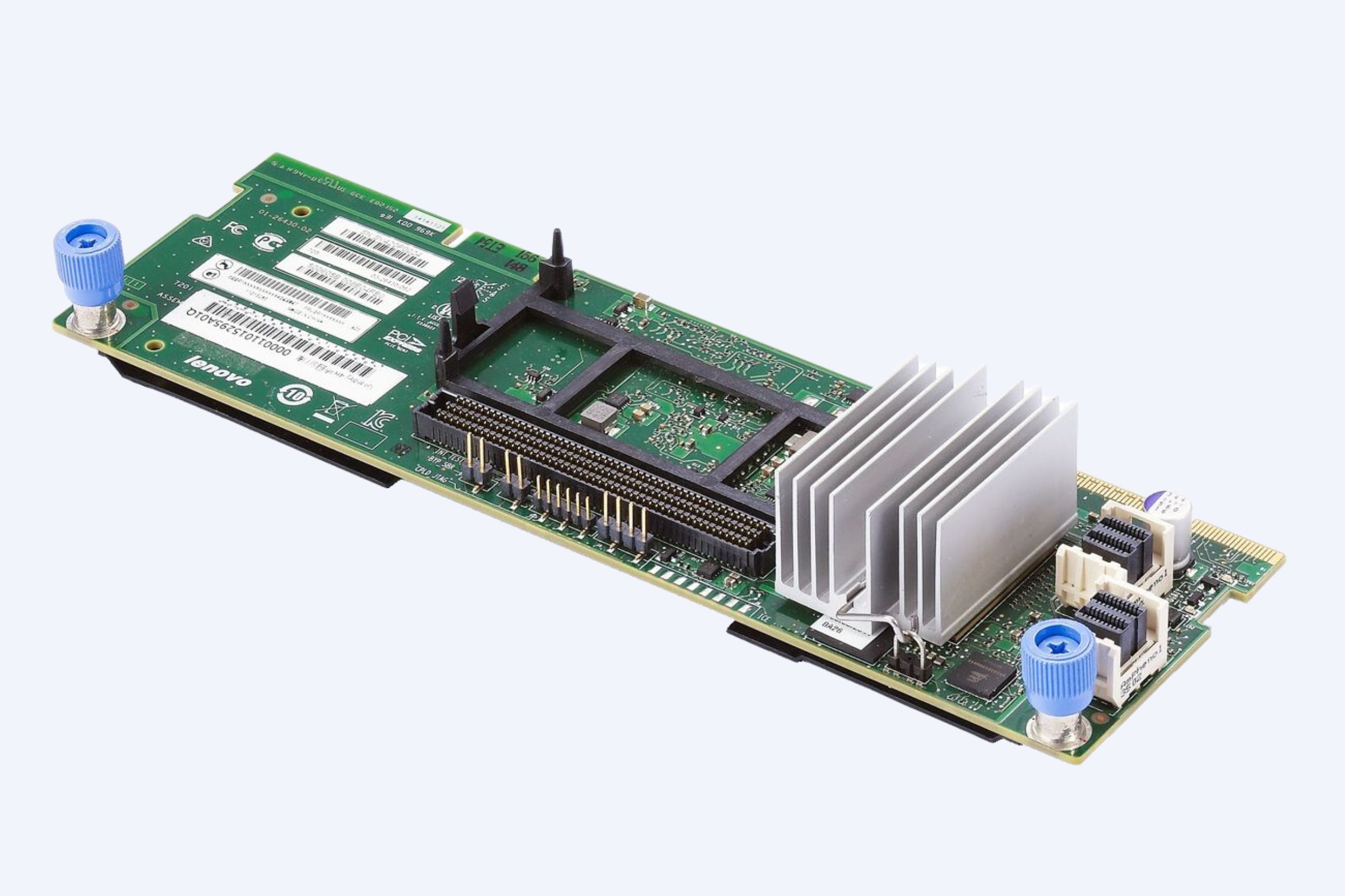
Wholesale Server Hardware ; IT Components Supplier ; Wecent
What is the architectural foundation of the MTIA v2 chip?
The MTIA v2’s architecture is built on a multi-core design with dedicated tensor processing cores and a unified memory subsystem. This foundation prioritizes high-throughput, low-latency inference for Meta’s diverse AI models, moving beyond general-purpose GPU limitations to achieve better performance-per-watt for targeted workloads.
At its core, the MTIA v2 employs a tiled architecture with numerous processing elements optimized for mixed-precision computations, crucial for modern inference. Each tile integrates scalar, vector, and tensor units, allowing it to handle the varied computational patterns found in recommendation models. The unified memory system, a critical departure from traditional GPU hierarchies, reduces data movement bottlenecks—a major source of power consumption. But what happens if the memory bandwidth can’t keep up with these specialized cores? The design addresses this with a high-bandwidth, on-chip network and likely leverages advanced packaging like 2.5D interposers to co-package HBM. For example, a single MTIA v2 chip might house 128 specialized tensor cores connected via a mesh network to 64GB of HBM2e, delivering over 1.5 TB/s of bandwidth. Practically speaking, this means a cluster of these chips can run complex ranking models with deterministic latency, which is vital for user feed generation.
The architecture isn’t just about raw compute; it’s a holistic system-level optimization for Meta’s software stack, from PyTorch down to the silicon.
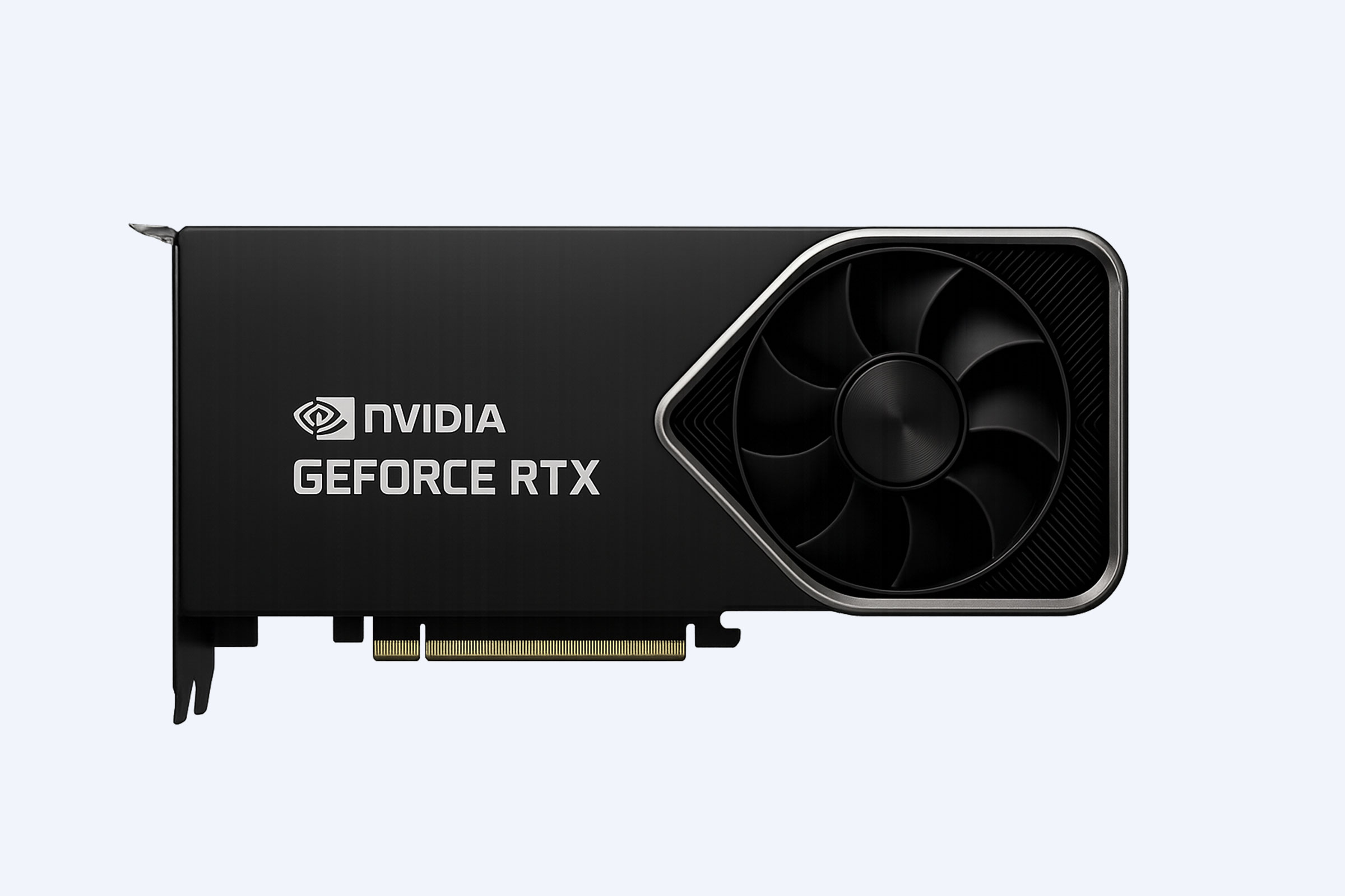
| Architectural Feature | MTIA v2 (Inferred Focus) | General-Purpose GPU (e.g., NVIDIA A100) |
|---|---|---|
| Core Design Philosophy | Fixed-function, inference-optimized tiles | Flexible, programmable SM (Streaming Multiprocessor) clusters |
| Memory Hierarchy | Unified, high-bandwidth on-chip/package memory | Complex multi-tier (L1/L2 cache, VRAM, system RAM) |
| Primary Optimization Goal | Performance-per-Watt for specific model families | Peak TFLOPS for diverse training & inference workloads |
How does MTIA v2 improve inference efficiency over GPUs?
MTIA v2 boosts inference efficiency through hardware-software co-design, minimized data movement, and precision optimization. By tailoring the silicon directly to Meta’s PyTorch models and eliminating general-purpose overhead, it achieves superior throughput and lower latency at a reduced total cost of ownership.
The efficiency gains are multifaceted. First, the co-design process ensures the compiler stack (like Glow or Meta’s own) can map model operations directly to the chip’s tensor cores with minimal translation overhead, unlike the driver and kernel layers of a GPU. Second, the unified memory architecture drastically cuts down on costly data shuffling between different memory pools. But is lower precision always the answer? MTIA v2 likely supports INT8, INT4, and even lower precision formats (FP8) that are sufficient for inference, allowing more operations per watt compared to the FP16/FP32 common in GPU training. For instance, running a recommendation model at INT8 on MTIA v2 could deliver a 3x improvement in queries per joule compared to running the same model on a GPU at FP16. Beyond raw silicon, the system-level integration—including custom networking and power delivery—further slashes overhead. Transitioning to deployment, this efficiency isn’t theoretical; it translates directly to lower operational expenses in Meta’s megascale data centers.
The result is a purpose-built engine that does one job exceptionally well, freeing up expensive, flexible GPUs for more varied tasks.
What are the key technical specifications of MTIA v2?
While full specs are proprietary, key inferred technical specifications include a 7nm or 5nm process node, high-bandwidth memory (HBM2e), and a multi-terabyte per second interconnect fabric. These specs are engineered to deliver massive parallelism and data throughput specifically for large-scale transformer and recommendation model inference.
Based on industry trends and Meta’s disclosures, we can extrapolate a likely specification profile. The process node is critical for density and power efficiency, with TSMC’s N7 or N5 being probable candidates. Memory is a cornerstone: expect 64-128GB of HBM2e per chip, providing the bandwidth needed to feed thousands of parallel operations. The interconnect fabric, perhaps a derivative of Open Compute Project (OCP) standards, enables scaling to thousands of chips within a single data center pod. So, how does this translate to real performance? A single MTIA v2 chip might deliver hundreds of TOPS (Tera Operations Per Second) at INT8 precision. For example, if it features 128 tensor cores running at 1.5 GHz, it could theoretically exceed 400 TOPS. In practical terms, this allows Meta to process billions of inference requests daily with predictable latency. Furthermore, the I/O subsystem is optimized for direct peer-to-peer communication, reducing host CPU dependency. This architectural choice is a game-changer for scaling out inference farms.
These specs aren’t just a list; they represent a calculated trade-off to build the most cost-effective inference machine for a defined workload set.
| Specification Category | MTIA v2 (Estimated) | Comparable GPU (NVIDIA A100 80GB PCIe) |
|---|---|---|
| Process Technology | 5nm/7nm (TSMC) | 7nm (TSMC N7) |
| Memory Type & Capacity | 64-128GB HBM2e | 80GB HBM2e |
| Peak INT8 TOPS | 400+ TOPS (inferred) | 624 TOPS |
| TDP (Thermal Design Power) | 150-250W (optimized for rack density) | 300W |
How is MTIA v2 integrated into Meta’s data center infrastructure?
MTIA v2 integration revolves around custom server chassis, tailored rack-scale power and cooling, and a software-defined network fabric. This holistic approach ensures the accelerators work as a cohesive, scalable unit within Meta’s Open Compute Project (OCP)-inspired data centers, maximizing resource utilization and minimizing latency.
Integration is where the rubber meets the road. Meta doesn’t just drop MTIA chips into off-the-shelf servers; they design custom motherboards and chassis that pack dozens of accelerators into a single rack unit, with optimized power delivery for high instantaneous loads. The cooling solution is equally critical, likely employing advanced direct-to-chip liquid cooling to handle the concentrated thermal output. But what about communication between thousands of these chips? A high-performance, low-latency network fabric—potentially leveraging Ethernet or a custom protocol—connects them, allowing models to be sharded across multiple accelerators seamlessly. For instance, a single recommendation request might be processed by a pipeline spanning four MTIA v2 chips across two different racks, all coordinated by Meta’s orchestration software. This level of integration demands deep vertical expertise, from silicon to system software. WECENT’s experience in deploying hyper-converged infrastructure for healthcare AI provides a parallel; ensuring low-latency paths between GPUs and NVMe storage was crucial for diagnostic imaging throughput.
The end goal is a data center that behaves less like a collection of servers and more like a single, gigantic computer dedicated to AI inference.

What software stack and tools support MTIA v2 development?
The MTIA v2 software stack is anchored by Meta’s deep PyTorch integration, a custom compiler toolchain (like Glow), and low-level kernel drivers. This stack allows developers to write models in standard PyTorch and have them efficiently compiled down to highly optimized code for the MTIA v2 hardware, abstracting away the silicon complexity.
The software journey begins with PyTorch, Meta’s flagship ML framework. Models are written as usual, but they can be tagged for MTIA execution. The Glow compiler (or a successor) then takes the computational graph and performs hardware-specific optimizations: operator fusion, memory allocation, and precision calibration. This compiler is the secret sauce, transforming flexible PyTorch code into a streamlined execution plan for the fixed-function tensor cores. But how do you debug performance on such a specialized platform? Meta likely provides profiling and debugging tools that offer insights into core utilization, memory bandwidth saturation, and kernel execution times. For a practical analogy, think of it like developing for a game console versus a PC; the fixed target allows for deeper optimization. WECENT’s support for NVIDIA’s CUDA stack in enterprise servers follows a similar principle—providing the full toolchain (NSight, Triton) is essential for client success.
The ultimate aim is to make the powerful hardware feel invisible to the data scientist, who simply sees faster iteration and lower inference costs.
What are the strategic implications of MTIA for the broader AI hardware market?
Meta’s MTIA v2 signals a major strategic shift towards vertical integration and workload-specific silicon, challenging the dominance of general-purpose GPU vendors. It underscores a future where hyperscalers design their own silicon to control costs, performance, and supply chains, potentially fragmenting the AI accelerator market.
The implications are profound. First, it demonstrates that for organizations with vast, predictable workloads, the economics of custom silicon can be favorable despite high R&D costs. This pressures GPU vendors to offer more specialized products or better pricing. Second, it accelerates innovation in interconnects, packaging, and memory architectures, as these become key differentiators. But will this trend trickle down to smaller enterprises? In the short term, likely not, due to the immense design and validation costs. However, it fosters a richer ecosystem of chiplet designs and open-source hardware initiatives that could eventually benefit the broader market. For example, Meta’s advancements in interconnect fabrics may feed back into OCP standards, improving efficiency for everyone. From WECENT’s vantage point in the supply chain, we see this creating a bifurcated market: hyperscalers with custom silicon and the vast majority of enterprises relying on commercial off-the-shelf (COTS) solutions from NVIDIA, AMD, and Intel. Our role is to guide clients through this complex landscape, ensuring they choose the right architecture—be it a fleet of H100 servers or a pilot deployment of alternative accelerators—for their specific business outcome.
The era of one-size-fits-all AI compute is ending, and MTIA v2 is a clear harbinger of that specialized future.
WECENT Expert Insight
FAQs
How does MTIA v2’s performance compare to an NVIDIA H100 for inference?
Direct comparisons are difficult, but MTIA v2 is optimized for Meta’s specific models and likely offers superior performance-per-watt and lower latency for those workloads, while the H100 retains superior generality and a mature software ecosystem for diverse AI tasks.
Does developing custom silicon like MTIA make Meta independent of NVIDIA?
Not completely. Meta will still rely on NVIDIA GPUs for many AI training workloads and for inference tasks outside MTIA’s optimization scope. It’s a strategy of diversification and optimization for core workloads, not a full replacement.
What does MTIA mean for enterprises buying AI servers from WECENT?
It reinforces the importance of workload analysis. We help clients choose between powerful, flexible GPU servers (like HPE with A100s) for mixed-use cases and more specialized, potentially cost-effective options as they emerge, ensuring infrastructure aligns with business goals.